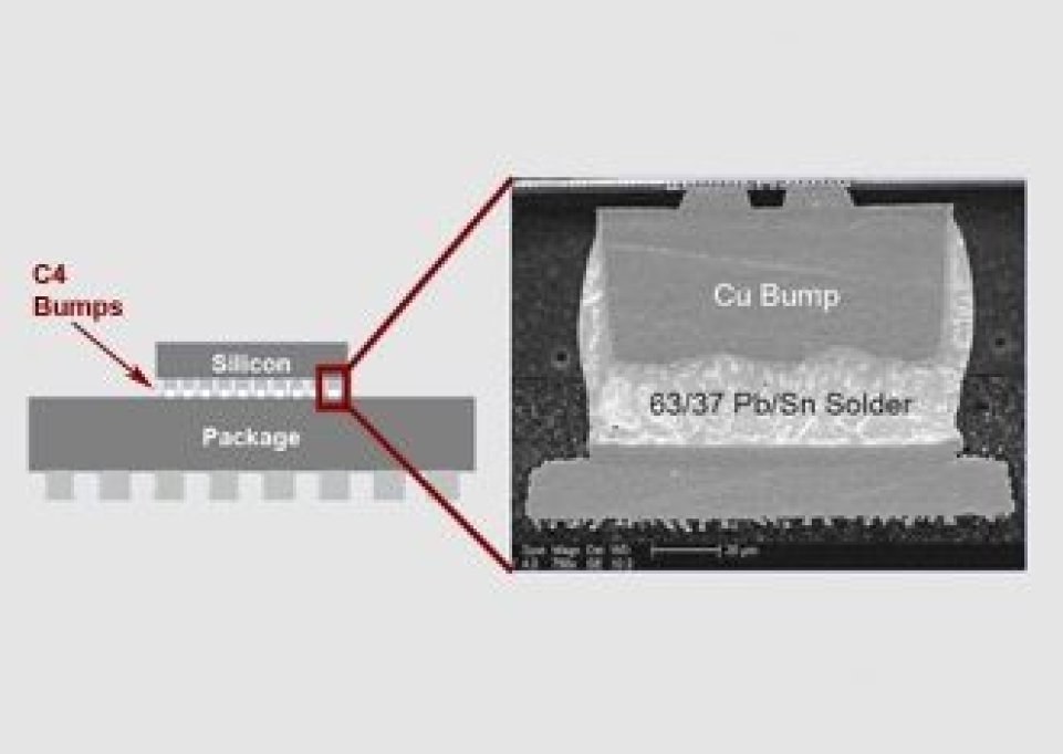
Die Bonding of Devices with Copper Pillar Bumps Application
Flip chip technology is keeping pace with the increasing connection density of the ICs and is capable of transferring semiconductor performance to the printed circuit board. The pitch is growing smaller, which means flip chip technology with solder bumps will unavoidably run up against its technical limitations. The reason for this is the spherical geometry of the bumps. The solution to this problem is copper pillars. In this contact technology for flip chip assembly, special cylindrical copper connections function with a solder deposit instead of the usual solder ball bumps to form the connecting element between semiconductor and substrate. The result: improved reliability and enhanced electrical and thermal connection characteristics, greater connection density with narrow pitching and RoHS conformity.

Examples of typical applications and products with CPB technology
Fine pitch ICs in extremely small housing forms for processors, fast memory components (DDR III), hearing aid and RFID solutions. Power MOSFETS requiring low resistance combined with thermal conductivity. High speed preamplifiers and RF modules requiring good thermal conductivity and high functional speeds. MEMS packages, due to large aspect ratios and stable bump geometries.
Any questions or interest in a online product demonstration?
Fabio Cocca - your sales contact at Dr. Tresky AG would be happy to talk to you personally. Give him a call or simply use our enquiry form.
+41 44 772 19 41
Please note our privacy policy.


